Jump to content
  • Intel says Ohio “megafab” will begin making advanced chips in 2025


    Karlston

    • 446 views
    • 7 minutes
     Share


    • 446 views
    • 7 minutes

    Intel will start with two fabs, but it has space for eight.

    Intel-Expansion-Ohio-2-800x518.jpg

    Intel's rendering of its two new leading-edge processor factories planned to be built outside Columbus, Ohio.
    Intel

    Intel announced the location of its megafab today, a 1,000-acre parcel on the outskirts of the Columbus, Ohio, metro area. The semiconductor manufacturer plans to break ground on two leading-edge fabs by the end of the year and enter production in 2025.


    “This is all part of the strategy that our CEO Pat Gelsinger announced back in March,” Intel Senior Vice President Keyvan Esfarjani told Ars.


    “We are starting with two fabs, and that’s all in line with the growing demand for what the industry needs,” he said. “It’s also critically important for the balance of the supply chain around the world.”


    Though the company will start with two fabs, the massive site gives Intel “optionality,” said Esfarjani, who oversees manufacturing, supply chain, and operations for the company worldwide. There’s room for up to eight fabs, “but we have space to do even more,” he said. If the entire site gets built out, Intel could spend as much as $100 billion on the Ohio site alone.


    image-1-640x360.png

    Intel's "megafab" will be located outside of the Columbus suburb of New Albany.
    Google Maps/Aurich

    Esfarjani said that Intel spent about nine months evaluating 35–40 locations across the US before settling on the New Albany parcel. The scale of the project demanded an entirely new site, he said. “All of our sites within the company, whether it’s in Oregon, New Mexico, or Arizona—we are essentially at the level where it’s not going to have enough footprint, enough space where you want to grow for those mega scales.”


    Gelsinger is betting that Intel can regain the lead in semiconductor manufacturing by making not just its own chips but chips for other companies, too. Traditionally, Intel has designed and manufactured chips for itself, but the success of foundries like TSMC, which focuses on making chips for others, has pushed Intel to open its fabs. In theory, making more chips will allow Intel to master new processes faster while giving it more cash to invest in the research and development of more advanced nodes. The new Ohio site will give Intel significant new manufacturing capacity, which Esfarjani said would be available to foundry customers, depending on demand.


    Intel-Expansion-Ohio-4-640x360.jpg

    The Intel site as it looks today.
    Intel

    While the company considered hundreds of variables, a few key factors helped influence the decision. First, Intel needed a location with the resources to support facilities of this size. The company required somewhere with ample land, water, and power. Second, it needed a metro area that could help supply enough technicians and engineers to run the fabs. And lastly, Intel was looking for state and local governments that would be eager to welcome the sites. (Amazon’s recent struggles with its HQ2 no doubt crossed Intel executives' minds.)


    “Out of all the options, Ohio—no brainer. It came to the top,” Esfarjani said. The farm fields around Columbus provided space to build and expand, while the region’s temperate climate offers a steady supply of water. (Esfarjani pointed out that the company recycles 95 percent of its water.) The state is also among the nation’s top 10 electricity producers, though nearly all of the power is generated by burning natural gas and coal. Intel intends for the site to be run on 100 percent renewable power, which will require the state to add significant wind and solar installations. “Part of why we are so anxious to move forward in announcing this project is so that we can formalize those engagements and get those agreements under way,” Esfarjani said.


    Intel will also be working with The Ohio State University and nearby community colleges to ensure a steady supply of technicians and engineers. Though the company isn’t releasing details of its educational plans yet, it did say it will spend $100 million supporting educational institutions, students, and the NSF to develop a pipeline for semiconductor jobs.

    Next-gen lithography

    The fabs are slated to open in the second half of 2025 and will support Intel’s then-current leading-edge process, which is likely to be Intel 18A. The node is expected to use gate-all-around transistors, which the company calls RibbonFET, and will be the first to use high-numerical aperture extreme ultraviolet lithography, also known as high-NA EUV. 


    Currently, only Netherlands-based ASML produces an EUV machine of any kind, and its high-NA EUV tools are expected to start making chips at the end of 2025, in line with Intel’s Ohio plans. Numerical aperture describes the ability of the system’s lenses to gather light and print finer features, and while the high-NA EUV isn’t ready for commercial production, it promises a 70 percent improvement in resolution. One of the biggest changes will be to the mirrors, which are made by Carl Zeiss. Because no material can be made transparent enough for EUV, today’s EUV scanners use mirrors instead of lenses. They’re made of alternating layers of molybdenum and silicon and are polished to a precision measured in atoms. For high-NA EUV, Zeiss will need to do that with larger, asymmetrical mirrors.


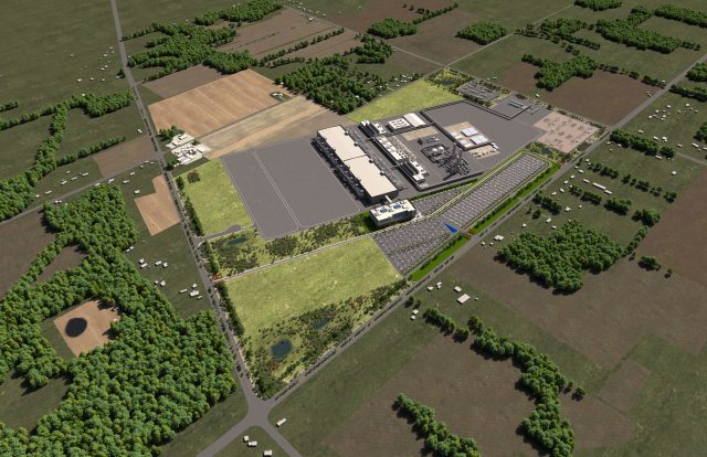
    Intel-Expansion-Ohio-5-640x414.jpg

    An aerial rendering of Intel's two new Ohio fabs.
    Intel

    Intel missed out on the first wave of EUV—competitor TSMC operates a majority of the EUV machines in existence, with Samsung using most of the rest—but it has placed an early bet on high-NA EUV in the hopes that it will be able to leapfrog the competition when the industry enters the 2 nm node (what Intel calls 20A).


    Earlier this week, Intel announced that it had submitted an order for the first production-ready high-NA EUV machine from ASML, due for delivery in 2025. It won’t be cheap—the Dutch company has said the first machines will cost “significantly” more than $340 million, more than double the cost of today’s EUV scanners. A fab running at full capacity will use more than a dozen of those machines.

    Costly endeavor

    Propping up a new leading-edge fab is costly no matter where it’s built, but the Semiconductor Industry Association, a trade group, estimates that building and running a fab in the US costs 25–50 percent more than elsewhere. That's why the SIA, Intel, and others have been pushing for Congress to pass the CHIPS for America Act, a $52 billion incentive to make more semiconductors in the US. Given today’s announcement, it’s no surprise that Ohio’s congressional delegation last week urged House and Senate leaders to fully fund the legislation.


    Intel estimates that building the two fabs will create 7,000 construction jobs, and once they’re up and running, the company will employ 3,000 people directly. Thousands more will likely follow as suppliers, including Applied Materials, LAM Research, Air Products, and Ultra Clean Technology, set up shop nearby.


    If the CHIPS Act is passed and funded, Esfarjani hinted that Intel’s plans for the site could be accelerated. “We’re very encouraged to see the bipartisan support for the CHIPS for America Act,” he said. “Partnership at not just the state level, but more importantly at the federal level, is going to be a strong catalyst to move a project like this forward even faster.”


    Intel says Ohio “megafab” will begin making advanced chips in 2025


    User Feedback

    Recommended Comments

    There are no comments to display.


    Join the conversation

    You can post now and register later. If you have an account, sign in now to post with your account.
    Note: Your post will require moderator approval before it will be visible.

    Guest
    Add a comment...

    ×   Pasted as rich text.   Paste as plain text instead

      Only 75 emoji are allowed.

    ×   Your link has been automatically embedded.   Display as a link instead

    ×   Your previous content has been restored.   Clear editor

    ×   You cannot paste images directly. Upload or insert images from URL.


  • Recently Browsing   0 members

    • No registered users viewing this page.
×
×
  • Create New...