AMD triples Zen 3 CPU cache using 3D stacking technology
Not a pipe dream—CEO Lisa Su demonstrated a working 3D-stacked 5900X prototype.

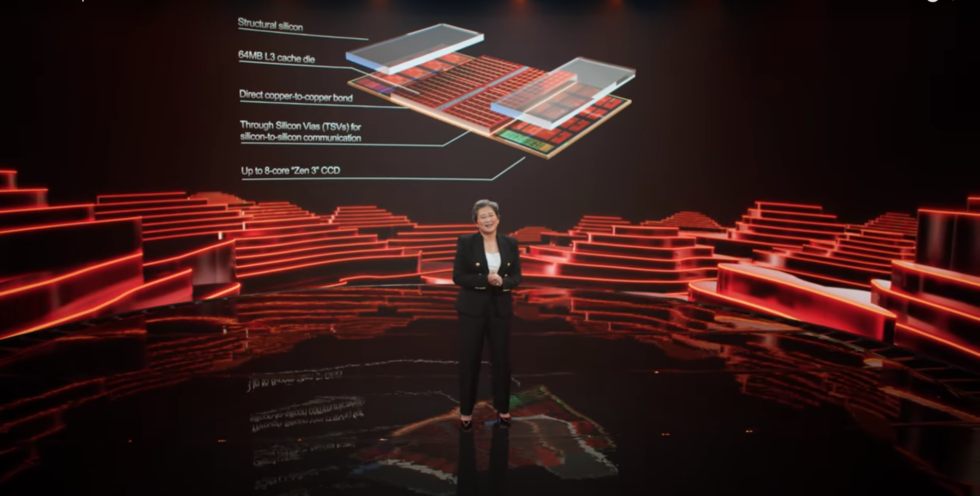
This exploded diagram shows an additional 64MiB of L3 cache atop the center of the CCD, with structural silicon inserts to either side of the new layer.

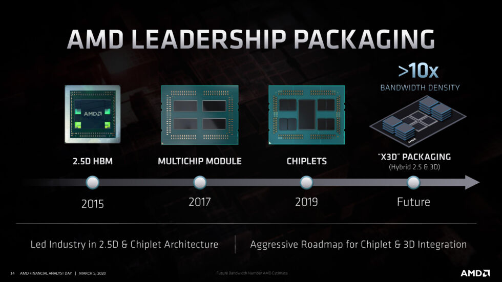
AMD teased X3D packaging in its Financial Analyst Day a few months ago, but the technology has reached production status much more quickly than expected.

AMD CEO Lisa Su holds up a delidded, 3D-stacked Ryzen 5900x processor on stage at Computex 2021.
Yesterday at Computex 2021, AMD CEO Lisa Su showed off the company's next big performance play—3D stacked chiplets, allowing the company to triple the amount of L3 cache on its flagship Zen 3 CPUs.
The technology is just what it sounds like—a layer of SRAM cache sitting atop the Complex Core Die (CCD) of the CPU itself. Current Zen 3 architecture integrates 32MiB of L3 cache per eight-core chiplet—making 64MiB total for a 12- or 16-core chiplet like the Ryzen 9 5900X or 5950X. The new technology adds an additional 64MiB L3 cache on top of each chiplet's CCD, bonded with through-silicon vias (TSVs).
The additional 64MiB L3 cache layer does not extend the width of the CCD, resulting in a need for structural silicon to balance pressure from the CPU cooling system. Compute and cache dies are both thinned in the new design, allowing it to share substrate and heat spreader technology with current Ryzen 5000 processors.


Tripling the L3 cache on Ryzen 5000 allows performance gains under some workloads—particularly archive compression/decompression and gaming—similar to those seen with entire new CPU generations. AMD demonstrated performance uplift via a Gears of War 5 demo. Paired with an unspecified GPU and with clock speed fixed at 4 GHz, a current-model 5900X system achieved 184 fps—while the triple-cached prototype managed 206 fps, a gain of roughly 12 percent.
AMD claims an average of 15 percent improved gaming performance with the new technology, ranging from a low of 4 percent for League of Legends to a high of 25 percent for Monster Hunter: World. This performance improvement requires neither smaller process node nor increased clock speed—which is especially interesting, in an era where clock speeds have largely hit a wall, and a physics-determined end to process-node shrink seems to be on the horizon as well.
Anandtech's Ian Cutress notes that AMD's new 3D chiplet stacking process is clearly TSMC's SoIC Chip-on-Wafer technology in action. While AMD is—at least so far—limiting itself to two layers, TSMC has demonstrated a full 12 layers in action. The problem here is thermal—adding RAM is a near-ideal use of the technology, since the additional silicon doesn't generate much in the way of additional heat. Stacking CPU on CPU would be far more problematic.
AMD states that the redesigned 5900X will enter production later this year—well before Zen 4's scheduled launch in 2022. For now, AMD is focusing on the new technology for "high-end Ryzen" CPUs only—no mention was made of Epyc, and the additional silicon required for the added cache makes it a likely nonstarter for budget processors, given current materials shortages.
Listing image by AMD
- vissha and aum
-

 2
2


3175x175(CURRENT).thumb.jpg.b05acc060982b36f5891ba728e6d953c.jpg)
Recommended Comments
There are no comments to display.
Join the conversation
You can post now and register later. If you have an account, sign in now to post with your account.
Note: Your post will require moderator approval before it will be visible.